The relentless march of Moore's Law has shaped the computing landscape for half a century. But as conventional silicon transistors approach atomic-scale dimensions, the industry faces a fundamental physical wall. Heat dissipation, quantum tunneling, and interconnect bottlenecks are placing hard limits on how much further we can push conventional electronics. Into this breach steps photonics — the technology of controlling and using light — offering a fundamentally different paradigm for high-performance computing.
What Are Photonic Chips?
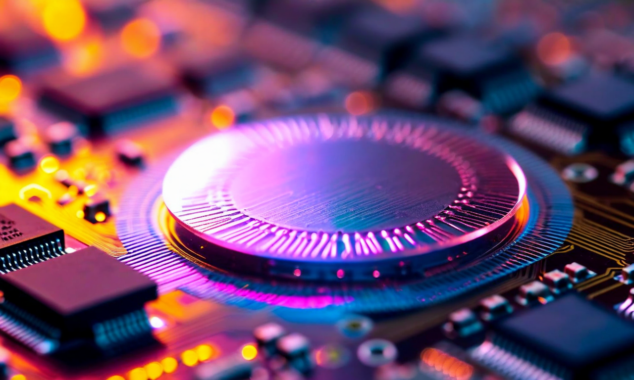
Photonic integrated circuits (PICs) are semiconductor devices that generate, detect, route, and process light on a single chip. Rather than moving electrons through resistive metal wires, they move photons through optical waveguides with extremely low loss and no heat generation from interconnect resistance. This distinction is profound: photons travel at the speed of light, do not interact with each other (enabling wavelength-division multiplexing), and can carry vastly more information per unit energy than electrons.
Modern photonic chips are fabricated on silicon or silicon nitride substrates using processes broadly compatible with conventional CMOS manufacturing, enabling co-integration with electronic circuits. A single chip might contain hundreds of optical components: waveguides, directional couplers, ring resonators, Mach-Zehnder interferometers, electro-optic modulators, and photodetectors — all operating on timescales measured in femtoseconds.
The Data Center Opportunity
The most immediate commercial application for photonic chips is optical interconnects in hyperscale data centers. As machine learning workloads scale up, the bandwidth requirements between compute nodes have grown explosively. A single AI training cluster may require petabit-scale interconnect bandwidth, and the energy cost of moving data between chips and across racks has become a dominant fraction of total system power consumption.
Silicon photonics transceivers operating at 400 Gbps, 800 Gbps, and even 1.6 Tbps per module are rapidly displacing electrical alternatives at distances beyond a few meters. Companies like Intel, Broadcom, and a growing ecosystem of photonics startups are investing heavily in this space, recognizing that photonic interconnects are not just an improvement over copper — they are a necessary enabler for next-generation AI infrastructure.
At Wove Photonic, we are targeting the next frontier: photonic computing, where optical components don't just carry data but actively process it. Matrix-vector multiplication — the computational bottleneck in deep learning inference — can be performed optically with near-zero energy cost, since light passing through a passive optical mesh performs the computation as it propagates. This is the fundamental physics advantage that motivates our work.
Optical Neural Networks
The concept of optical computing is not new — researchers have explored it since the 1960s. But it is the convergence of modern photonic integration capabilities, deep learning workload growth, and advances in programmable optical elements that has made it commercially viable. An optical neural network processes information by encoding data as the amplitude or phase of light, passing it through a network of configurable optical elements that implement the weights of a neural network, and reading out the result with photodetectors.
The efficiency advantage is substantial. A single photonic chip performing a matrix-vector multiply operation consumes orders of magnitude less energy than an equivalent GPU or ASIC implementation, because the optical computation itself is essentially passive — it leverages fundamental properties of wave propagation rather than electronic switching. Latency is also reduced, as computation occurs at the speed of light traversal through the chip.
Photonic computing is not about replacing all of computing with light. It is about finding the operations where photons have a decisive advantage over electrons — and matrix multiplication in neural networks is the clearest such case today.
Manufacturing Challenges
The path from laboratory proof-of-concept to manufacturable photonic computing chips is technically demanding. Achieving the fabrication precision required for consistent optical performance requires tolerances measured in nanometers. Thermal drift, fabrication variations, and coupling losses must all be managed within tight specifications. The industry has made substantial progress on these challenges over the past decade, benefiting from investments by hyperscaler companies and semiconductor manufacturers who recognize the strategic importance of photonic integration.
At Wove Photonic, we have developed a silicon nitride platform specifically optimized for the demanding requirements of photonic computing. Our proprietary waveguide designs achieve propagation losses below 0.1 dB/cm, enabling complex photonic circuits with hundreds of components without unacceptable signal degradation. Our fabrication process has been validated at a leading silicon photonics foundry and is ready for scale-up.
The Road Ahead
The photonic computing market is at an inflection point. Several well-funded startups — Lightmatter, Lightelligence, Luminous Computing, and others — are racing to deliver the first commercial optical neural network accelerators. Cloud providers and AI hardware companies are watching closely, recognizing that whoever solves the energy efficiency challenge at scale will command enormous commercial advantage.
The trajectory is clear: photonic chips will play an increasingly important role in the compute infrastructure that powers the AI era. The question is not whether photonics will reshape computing, but when, and which teams will crack the remaining engineering challenges first. At Wove Photonic, we believe that answer is close, and we are working to be at the forefront of that transition.